Photovoltaics based on Copper oxide
Photovoltaics based on Copper oxide
Preparation and Characterization of Optoelectronic Materials using Scanning Tunneling Microscopy and Luminescence Spectroscopy

Principal investigator: Prof. Dr. Niklas Nilius
collaboration: Prof. Dr. Katherina Al-Shamery, Prof. Dr. Thorsten Klüner
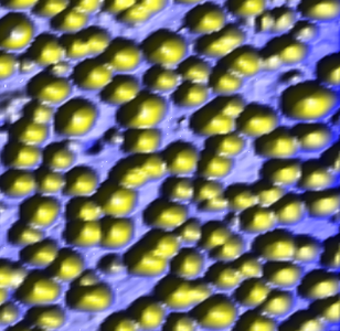
Copper-based sulfide and oxide materials are in the focus of intense research activities with the aim to fabricate a new generation of cheap and robust photovoltaic devices. Common routes to enhance the efficiency in the light-to-energy conversion include a better morphological control, for instance by improving the crystallinity, as well as targeted modifications of the electronic structure, e.g. by altering the stoichiomtry and incorporating dopant ions. In this work, we attempt to grow crystalline copper oxide and sulfide layers on different metallic and dielectric supports. The films will be prepared by physical vapor deposition in an ultra-high vacuum environment. The growth will be characterized from the structural and morphological point of view, using electron diffraction and scanning tunneling microscopy. Chemical analysis is achieved by photoelectron spectroscopy, whereas low-temperature tunneling spectroscopy will be used for an electronic characterization. The identification of point and line defects in the oxide and sulfide lattices will be a major aim of this work, as their parasitic effects are often made responsible for the low conversion cross section of a device. Finally, an optical characterization of the copper-based films will be realized with a confocal laser microscope, enabling spatially resolved measurements with sub-micron resolution. By optimizing all relevant preparation steps and characterizing the resulting systems down to the atomic scale, we hope to advance the behavior of copper-based materials in photovoltaic applications.


