Nanoscale 3D printing
Nanoscale 3D printing
Nanoscale 3D printing
Additive manufacturing of metallic structures at the micro- and nanoscale is currently a rapidly developing research area. In general, 3D printing techniques can be classified into methods that rely on the transfer of pre-synthesized material and approaches using localized synthesis (deposition) of metals in situ. The former class of methods typically utilizes metal nanoparticles that are brought onto the substrate by direct ink writing,1 electrohydrodynamic printing,2 electrophoresis3 or nanoparticle trapping.4 Often, post-printing steps, e.g. for particle sintering, are included in the fabrication procedures and in some cases the final performance of the printed features is affected by these post-printing treatments.
The other family of AM methods is based on in situ metal fabrication that is the conversion of precursor species into solid metal using electron or ion beams,5 local photochemical reactions,6, 7 or electrochemical techniques. These methods generally exhibit higher printing resolution since there is no need to manipulate objects, like particles, or large volumes of inks, result in fully dense structures with superior mechanical and electrical properties and also offer wider range of printing materials. Electrochemical techniques are particularly advantageous for micro- and nanoscale AM due to their intrinsic simplicity, high degree of control over the morphology of the resulting features, and the potential for automation.
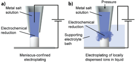
Recently, several electrochemical methods have been introduced for metal AM at sub-micrometer scale. The key principle that underlies these techniques is based on the confinement of electrodeposition using localized delivery of precursor species or performing an electrochemical reaction in a small volume on the substrate using a droplet cell (see Figure 1). The former family of approaches is based on electroplating of locally dispensed ions in liquid, where metal ions are delivered with a nanopipette. Metal ions are locally introduced using a pressure-driven flow8, 9 or by electromigration from a nanopipette tip,10 which is precisely positioned and kept at a certain distance from the printed feature by using force- or ion current feedback. Another family of electrochemical 3D printing techniques is based on electrodeposition, which is confined within a liquid meniscus formed between a capillary tip and a substrate,11-14 enables printing with ca. 300 nm critical dimension.13 Other emerging techniques, like a recent redox hydrodynamic printing bring further advantages of a multimaterial printing with high resolution approaching 100 nm mark.15
Our goal is to bring 3D printing of materials, such as conductors and semiconductors, to a true nanoscale (<100 nm), where a variety of applications become immediately available. Additive manufacturing at this dimension opens up new pathways for making sensing interfaces, nanomechanical systems, nanorobots, as well as nanoelectronic devices to attain unprecedented performance. This requires new approaches for 3D printing, smaller nozzles, advanced local delivery methods, as well as high-end hardware and software capable to achieve the desired architectures. Another major challenge is the typically low printing rates, which should improve by about orders of magnitude to connect nano-interfaces with the real-world problems. Our group is constantly working on pushing the capacity of nanoscale 3D printing techniques to the new level.
References
1. Ahn, B. Y.; Duoss, E. B.; Motala, M. J.; Guo, X.; Park, S.-I.; Xiong, Y.; Yoon, J.; Nuzzo, R. G.; Rogers, J. A.; Lewis, J. A. Omnidirectional Printing of Flexible, Stretchable, and Spanning Silver Microelectrodes. Science 2009, 323, 1590.
2. Galliker, P.; Schneider, J.; Eghlidi, H.; Kress, S.; Sandoghdar, V.; Poulikakos, D. Direct Printing of Nanostructures by Electrostatic Autofocussing of Ink Nanodroplets. Nat. Commun. 2012, 3, 890.
3. An, S.; Jhe, W. Nanopipette/Nanorod-Combined Quartz Tuning Fork–Atomic Force Microscope. Sensors 2019, 19.
4. Takai, T.; Nakao, H.; Iwata, F. Three-Dimensional Microfabrication Using Local Electrophoresis Deposition and a Laser Trapping Technique. Opt Express 2014, 22, 28109-28117.
5. Fisher, J. S.; Kottke, P. A.; Kim, S.; Fedorov, A. G. Rapid Electron Beam Writing of Topologically Complex 3D Nanostructures Using Liquid Phase Precursor. Nano Lett. 2015, 15, 8385-8391.
6. Yee, D. W.; Lifson, M. L.; Edwards, B. W.; Greer, J. R. Additive Manufacturing of 3D-Architected Multifunctional Metal Oxides. Adv. Mater. (Weinheim, Ger.) 2019, 0, 1901345.
7. Vyatskikh, A.; Delalande, S.; Kudo, A.; Zhang, X.; Portela, C. M.; Greer, J. R. Additive Manufacturing of 3D Nano-Architected Metals. Nat. Commun. 2018, 9, 593.
8. Hirt, L.; Grüter, R. R.; Berthelot, T.; Cornut, R.; Vörös, J.; Zambelli, T. Local Surface Modification via Confined Electrochemical Deposition with FluidFM. RSC Adv. 2015, 5, 84517-84522.
9. Hirt, L.; Ihle, S.; Pan, Z.; Dorwling-Carter, L.; Reiser, A.; Wheeler, J. M.; Spolenak, R.; Vörös, J.; Zambelli, T. Template-Free 3D Microprinting of Metals Using a Force-Controlled Nanopipette for Layer-by-Layer Electrodeposition. Adv. Mater. (Weinheim, Ger.) 2016, 28, 2311-2315.
10. Momotenko, D.; Page, A.; Adobes-Vidal, M.; Unwin, P. R. Write–Read 3D Patterning with a Dual-Channel Nanopipette. ACS Nano 2016, 10, 8871-8878.
11. Hu, J.; Yu, M.-F. Meniscus-Confined Three-Dimensional Electrodeposition for Direct Writing of Wire Bonds. Science 2010,329, 313.
12. Daryadel, S.; Behroozfar, A.; Morsali, S. R.; Moreno, S.; Baniasadi, M.; Bykova, J.; Bernal, R. A.; Minary-Jolandan, M. Localized Pulsed Electrodeposition Process for Three-Dimensional Printing of Nanotwinned Metallic Nanostructures. Nano Lett. 2018, 18, 208-214.
13. Lin, Y.-P.; Zhang, Y.; Yu, M.-F. Parallel Process 3D Metal Microprinting. Adv. Mater. Technol. (Weinheim, Ger.) 2019, 4, 1800393.
14. Lei, Y.; Zhang, X.; Xu, D.; Yu, M.; Yi, Z.; Li, Z.; Sun, A.; Xu, G.; Cui, P.; Guo, J. Dynamic “Scanning-Mode” Meniscus Confined Electrodepositing and Micropatterning of Individually Addressable Ultraconductive Copper Line Arrays. J. Phys. Chem. Lett. 2018,9, 2380-2387.
15. Reiser, A.; Lindén, M.; Rohner, P.; Marchand, A.; Galinski, H.; Sologubenko, A. S.; Wheeler, J. M.; Zenobi, R.; Poulikakos, D.; Spolenak, R. Multi-Metal Electrohydrodynamic Redox 3D Printing at the Submicron Scale. Nat. Commun. 2019, 10, 1853.