Microwave Nanoscopy
Contact
Microwave Nanoscopy
Research on “beyond CMOS” requires smart tools to investigate, manipulate and transport materials, objects and systems in the nanoscale range. One crucial part along these track is imaging and characterizing the electric and dielectric properties in the microwave region of the electromagnetic spectrum. With our nanorobotic approach we working on new instruments measuring electric/dielectric parameters, like our novel in-situ Scanning Microwave Microscope.

Fig.: Scanning Probe Microscopy techniques in the frequency spectrum
In-situ near-field probing
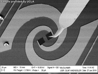
The selfdeveloped laserinterferometer-based Scanning Microwave Microscope is integrated into a Scanning Electron Microscope (SEM2). This world-first technology allows in-situ measurements on nanoelectronic and heterogeneous nanoscale objects. Precise positioning of an RF probe, scanning the region-of-interest, is necessary to ensure high repeatability of the high-frequency measurements. Additionally, we investigate the necessary automation and calibration methods. Infos: Olaf C. Haenssler.
SEM2 Video
Control and data processing

High-performance hardware and software solutions are increasingly required for recording, measuring and processing the data that is generated. Due to a high number of sensors and the need to combine different measuring devices, the synchronization of different electronic components is important.
For this purpose, we are developing solutions .
The hardware requirements are often so time intensive that embedded systems based on Field Programmable Gate Arrays (FPGAs) with powerful co-processors are used. These can process the data at high speed. This is achieved by modeling parts of this processing chain as hardware modules. These systems then work directly on the data stream of the sensors or measuring devices and can process data in parallel.
Furthermore, various interfaces are often required to implement communication between the sensors and measuring devices. A subsequent field of microwave nanoscopy is the processing and presentation of the data obtained as measurement images to represent objects and their properties in orders of micro- and nanometres. In addition to displaying the images, further analysis and processing of the recording is an issue in this context. In addition to the recording of the data, the actuation of the scanning microwave microscope on the basis of various scanning methods play a role.
Projects
On international level, Olaf C. Haenssler organized special sessions at MARSS conference in Montréal, Nagoya and Helsinki.


Current Active Projects
- "Fast Broadband Scanning Microwave Microscopy", DFG
- "mm-Wave Dynamic Metasurface Reflectorswith independent Amplitude-Phase Control using electronically-tunable Graphene (MdmReg)", DAAD, Cooperation with Metamaterials & Antenna Research Squad at Carleton University, Ottawa, Canada (2022-24)
Completed Projects
- "Fusion of Integrated Near-field Optoelectronic Scanning Probe Microscopy with Electron Microscopy", DAAD, Cooperation with NIST, Boulder, CO, USA (2019-21)
- "Liquid contact probing", DFG
- "VACSMM for quantitative Characterization of sub-10nm and aF scale Capacitors and Memories", DFG-ANR, Cooperation with the Micro and Nano Systems Group at the CNRS-Institut d’Electronique, de Microélectronique et de Nanotechnologie, Lille, France
- "Graphene-based Microwave Components", DAAD-PROCOPE, Cooperation with IEMN / CNRS UMR 8520, Lille, France
- "MEMS-based Scanning Microwave Microscope Integration into a Nanorobotic Environment under Vacuum", DAAD, Cooperation with Centre for Integrated RF Engineering (CIRFE) at University of Waterloo, Canada (2016-17)
- "Nanorobotic-assisted Scanning Microwave Microscopy to analyze and manipulate 2D- and Biomaterials", DAAD-MIUR, Cooperation with Department of Information Engineering at Università Polytecnica delle Marche, Ancona, Italy (2016-17)
- "Calibration standard and Nanoautomation of a SMM-in-SEM", DAAD-IKYDA, Cooperation with the Micro-/Nanoelectronics Group at Foundation for Research and Technology-Hellas (FORTH-IESL), Iraklio, Greece (2015-16)
- "Extending AFM nanocharacterization capabilities: automated assembly of CNT AFM tips and development of scanning microwave microscopy methods", DAAD-PROCOPE, Collaboration with the NAM6 group at IEMN / CNRS UMR 8520, Lille, France (2013-14)