Scanning Electrochemical Microscopy (SECM)
Contact
Mailing Address
Visitors
Scanning Electrochemical Microscopy (SECM)
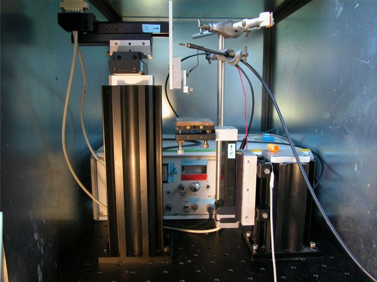
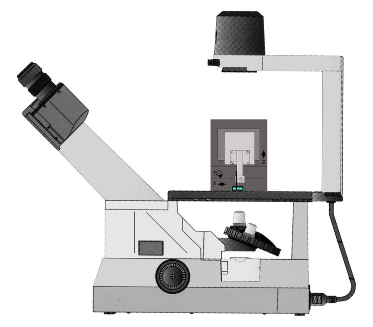
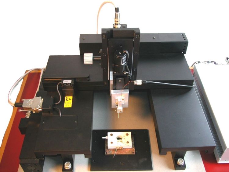
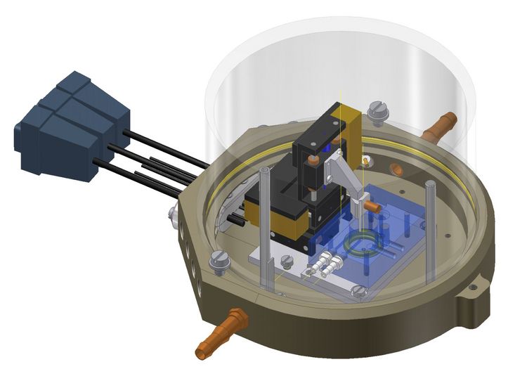
Instrumentation
The instrumentation for SECM is developed in our group based on commecial components. The isntriments are controlled by our own software for data acquisition and data evaluation. This allows us to adapt the setup and measurement routines to different scientific problems.
Method
Scanning electrochemical microscopy (SECM) is a scanning probe technique similar to AFM and STM. The particular feature of SECM is the chemcial nature of the recorded signal. It is caused by the electrochemcial conversion (electrolysis) of a dissolved compounds (often called mediator in the context of the method) at an microelectrode, whose sidewalls are completely covered by a insulating layer. The experiment is designed in a way, that the number of converted mediator species at the microelectrode depends on the chemcial reactions occuring on the sample. A plot of the microelectrode current vs. lateral coordinates provided a mapping of the chemical reactivity of the sample.
We use the method for very different application; this includes the following area
- Investigation of interfaces in batteires and other electrochemcial energy conversion devices
- Imaging of biochemically active layers
- Development of coupling techniques with other scanning probe techniques
- Local surface modification
- Digital simulationen of the SECM imaging process
Review paper about the method: G. Wittstock, M. Burchardt, S. E. Pust, Y. Shen, C. Zhao
Scanning Electrochemical Microscopy for Direct Imaging of Reaction Rates
Angew. Chem. Int. Ed. 2007, 46, 1584-1617. Abstract & Link
Working principle
The basic principle of the method can be explained using the investigation of a microelectrode array. The microelectrode array was produced by thick film technology. A graphite layer was covered by an insulating polymer film. Individual electrodes were formed by laser ablation of the insulating cover layer. One has to check whether the „holes” in the cover layer are deep enough to complete penetrate through the graphite layer. An image by scanning electron microscopy (SEM) shows the shape of the „holes” but does not provide a conclusion whether the graphite layer has really been exposed. Scanning electrochemical microscopy shows the individual electrode on the sample by high currents because the chemcial reaction occurs there. This allows to distinguish clearly between „holes” that yield a functioning electrode and those that do not expose the graphite layer.
Sample: Development sample of Senslab GmbH
All scientific details: B. Gründig, B. Strehlitz, K. Zimmer; Evaluation of Microelectrode Arrays for Amperometric Detection by Scanning Electrochemical Microscopy. Electroanalysis 1998, 10, 526-531. Abstract & Link


