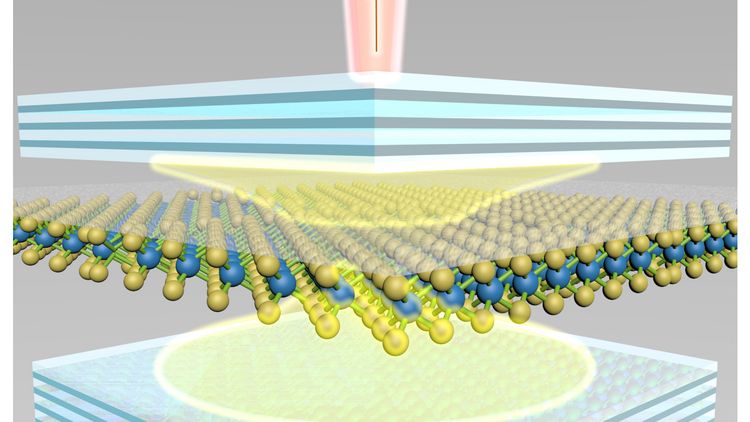


When crystals consist of only a single layer, they often exhibit strange properties. The Quantum Materials working group at the Institute of Physics is making the two-dimensional semiconductors glow - a first step towards future, tiny laser light sources.
The raw material for future nanolasers looks similar to aluminium foil and is contained in a thin glass tube. Dr Carlos Antón-Solanas holds the tube up to the light so that the tiny, shiny metallic flake inside can be seen at all: a piece of the semiconductor tungsten diselenide. The sample is smaller than a fingernail and much thinner than a human hair. However, the physicist needs much, much thinner layers of the material for his experiments. "Tungsten diselenide has interesting optical properties - but only if you use a single layer of this crystal," says the physicist.
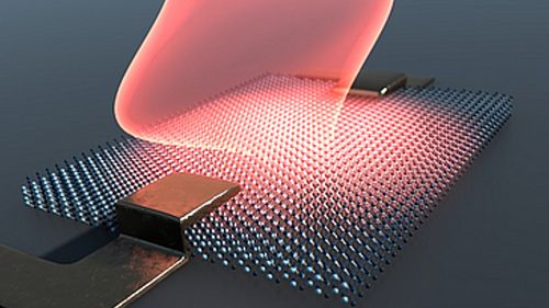
Antón-Solanas and the other researchers in the Oldenburg Quantum Materials working group led by Prof. Dr Christian Schneider are experimenting with so-called two-dimensional materials - solids that are often less than a billionth of a metre (nanometre) thick. The physicists' aim is to better understand the interaction of light and matter in these unusual materials. They are also working on transforming the 2D crystals into tiny light sources. When the semiconductors are excited in a certain way, they emit laser light: electromagnetic radiation that is monochromatic, i.e. only has a single wavelength, and which propagates in a specific direction. In addition, the emissions can be superimposed with other light waves in such a way that interference occurs.
Transmitting information with light
This light, known as "coherent" in physics, is suitable for transmitting information in tiny circuits. Tiny lasers could connect optical and electronic components in future chips. This type of technology could drastically increase the data transmission and computing power of processors. "Applications in this area have the potential to influence our daily lives," says Schneider. He is researching 2D crystals as part of the UnLiMIt-2D (Unique Light-Matter Interaction with Two Dimensional Materials) project, which is being funded by the European Research Council (ERC) with a "Starting Grant".
Schneider and his team of researchers have already taken the first steps on their journey: They recently reported in the journal Nature Communications that they had made a sample of tungsten diselenide emit laser radiation at room temperature. Previously, they had only been able to generate comparable effects in a vacuum and at temperatures just above absolute zero. "The transition from these cryogenic temperatures to room temperature means that two-dimensional materials are becoming really interesting for applications," says Schneider, who has been conducting research at the University of Oldenburg since mid-2020.
Quantum materials and liquid light
The unusual physical properties of the 2D crystals are primarily due to the electrons, which behave completely differently within the wafer-thin layers than in thicker solids. Because the laws of quantum theory play an important role in these materials, experts also refer to the two-dimensional solids as "quantum materials". In tungsten diselenide and related semiconductors, for example, the electrons can be made to combine with light particles for a short time to form a kind of hybrid of light and matter. The resulting physical objects are sometimes referred to as liquid light. They have both the properties of electrons and the properties of light - an unusual combination from a physical point of view. What is particularly interesting is that if the number of particles is large enough, they merge to form what the researchers call a "macroscopic quantum state". The particles then behave as if they were a single particle. When this transformation takes place, the thin crystals begin to emit more laser light. It is precisely this phenomenon that Schneider and his team are investigating.
In the material they are currently investigating, the semiconductor tungsten diselenide, a crystal layer consists of three layers of atoms. Like in a sandwich, a layer of tungsten atoms lies between two layers of selenium atoms. Because the individual crystal layers in this material - similar to the carbon compound graphene, for example - are only weakly connected to each other by electrostatic forces, they can be easily separated from each other.
Sellotape as the most important tool
A specialist in peeling even thinner crystal layers from the already thin samples is Dr Bo Han, a postdoctoral researcher in the Quantum Materials working group. His colleagues call him a "quantum artist". His most important tool: scotch tape. "You put a piece of tungsten diselenide between two pieces of tape, pull them apart again and repeat this over and over again," he explains. In this way, he gradually succeeds in peeling off thinner and thinner layers - until hopefully at some point a single layer sticks somewhere on the adhesive tape, which Han recognises due to certain light reflections. The physicists then confirm the discovery under the microscope. Even there, the thin layers are only recognisable to specialists - they are almost transparent and only just stand out as a thin veil against the background.
In order to transform the two-dimensional semiconductors into tiny lasers, the researchers are working together with colleagues all over the world. The samples themselves come from co-operation partners of the team at the University of Arizona in the USA. The researchers then cover their samples with a protective layer of the diamond-like material boron nitride, which they receive from colleagues at the National Institute of Materials Science in Tsukuba, Japan. The shreds are then placed between two special mirrors provided to the team by colleagues from the Universities of Jena and Würzburg.
Tiny lasers in view
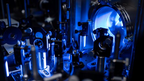
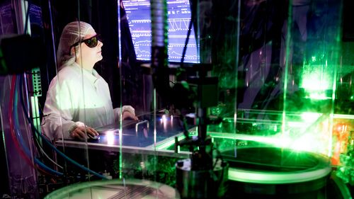
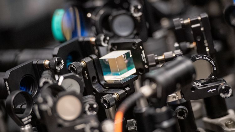
The team can then analyse the light emissions from the thin semiconductors. The experiments take place in a laboratory on the first floor of the main building on the Wechloy campus. "We are currently still setting up the lab, but we got it up and running in record time," reports Antón-Solanas. All kinds of optical devices are set up in the darkened room: Lenses, semi-transparent mirrors and spectrometers that can analyse light. There is also the rhythmic sound of a pump that cools liquid helium to temperatures close to absolute zero. The team also continues to carry out experiments at extremely low temperatures, where some materials can be brought to the desired quantum state more easily.
The fact that many experiments can now also take place at room temperature makes the researchers' work much easier. They are currently investigating how the emissions from the tiny lasers can be controlled even more precisely: Using external electrical fields or mechanical stresses, for example, it could be possible to change the colour of the radiation as well as its quantum statistical properties - which in turn opens up new potential applications.