Hydrogen Production
Contact
Mailing Address
Visitors
Hydrogen Production
Combinatorial Testing of Photoelectrocatalysts for Water Splitting
by Svenja Speldrich
Photoelectrochemical water splitting is a potential dream reaction for sustainable hydrogen production using sunlight. The first demonstration of a TiO2 photoanodedates back to 1972 and led to intensive research in this field. Today, there is no large-scale process for photoelectrochemical H2 production due to low cell efficiencies.
The key to success lies in a semiconductor electrode material that meets all of the following conditions:
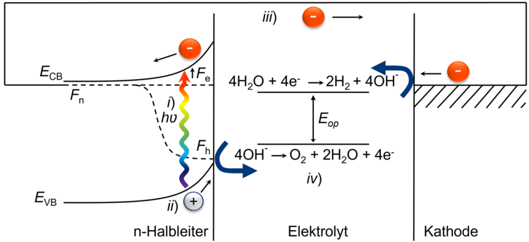
i) Suitable band gap for absorption of sunlight
(ii) Matching band edges for the half-cell reactions of the oxygen evolution reaction (OER) and hydrogen evolution reaction (HER)
iii) High light absorption coefficient
(iv) High photovoltage with rapid charge transfer
v) Stability under oxidizing or reducing conditions
(vi) Low-cost manufacturing processes, abundant and non-toxic starting elements (frequent natural occurrence).
The above-mentioned conditions suggest more complex materials, which are composed of several elements, so-called multi-component materials.
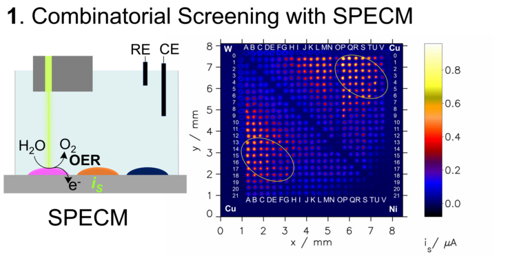
Before different materials are examined in elaborate individual tests (batch experimentation), it makes sense to carry out a combinatorial study of a wide variety of elements. In combinatorial testing, different elements in different compositions (so-called material libraries) are combined in a high-throughput process and functionally tested. Only the most active compositions are then further investigated in more detail in batch experimentation. A widely used approach for producing material libraries is ink-jet printing followed by calcination, in which a special material printer is used to produce predefined patterns of different materials. Different layouts for binary, ternary and quaternary element mixtures can be printed in the form of separate dots (spots), each spot having a specific composition. In addition, it is possible to produce layered materials through repeated printing and calcination. The possibility of layer-by-layer printing allows the application of additional catalysts, formation of heterostructures or protective layers.
A rapid functional characterization, in terms of photoactivity, is scanning electrochemical probe microscopy using light as a probe. This modification of classical scanning probe microscopy is abbreviated as SPECM from scanning photoelectrochemical microscopy (Figure 2). Here, a selected wavelength range is used to locally illuminate the spots and the photocurrent for the illuminated area is measured in a three-electrode setup. By scanning with the light probe, material spots with different compositions are illuminated one after the other and the photocurrent generated in each case is combined to form a photoactivity map of the material library. The evaluation of such maps shows so-called hit compositions, which are then further analyzed structurally in detail.
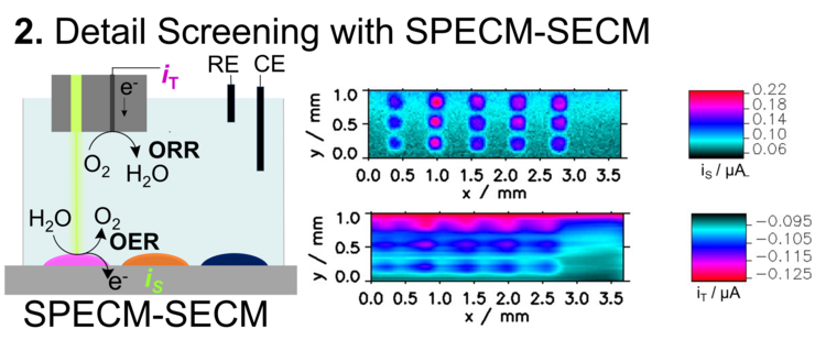
Another form of scanning probe technology with a probe combining an optical fiber and a platinum microelectrode allows simultaneous measurement of oxygen evolution reaction (OER) at the illuminated spot and oxygen reduction reaction (ORR) from the formed oxygen at the Pt microelectrode (Figure 3). This detection is important because photocurrents can also result from (unwanted) photocorrosion of the absorber material, which is not detectable by a single SPECM measurement. The combined method requires longer measurement times due to slow stepping speed between two spots. Therfore, this method is often used only for selected metal oxide compositions.
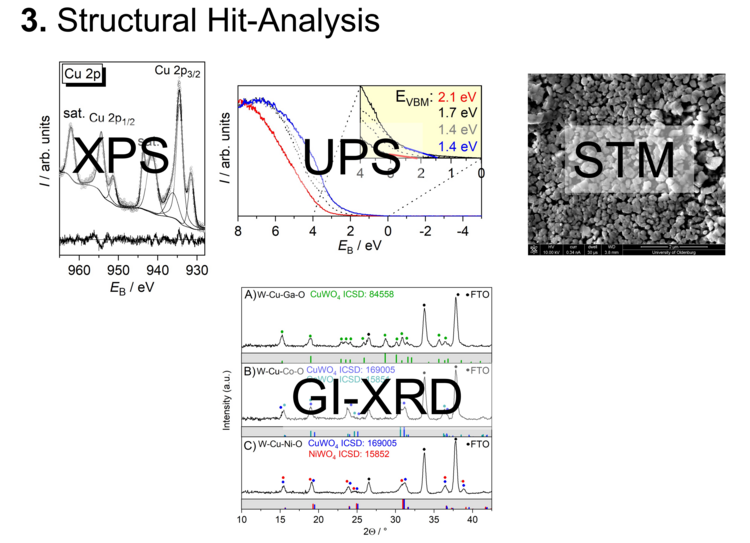
The printed samples for the SPECM measurements are performed at approximately 8 mm × 8 mm size, since the readout times become too long for larger samples. A sample of this size covers here over 550 different compositions (100-200 µm diameter for each spot). For a subsequent structural characterization of the most active spots, samples with larger spots are printed. For structural elucidation, for example, XPS, UPS, XRD, Raman spectroscopy, and STM are suitable (Figure 4).
Own contribution to the field
- S. Speldrich; M. Wark, G. Wittstock
Metal Oxide Protection Layers for Enhanced Stability and Activity of WO3 Photoanodes in Alkaline Media
ACS Appl. Energy Mater. 2023, 6, 9602-9614 Abstract and Link (open access) - S. Speldrich, L. Gronewold, M. Wark, G. Wittstock
Enhanced Photoactivity by Doping of Cu-W Oxide-Based Photoanodes by Trivalent Al3+, Ga3+ and In3+ Ions – A Combinatorial Study
ACS Appl. Eng. Mater. 2023, 1, 3284-3297 Abstract & Link (open access) - S. Baues, H. Vocke, L. Harms, K. K. Rücker, M. Wark, G. Wittstock
Combinatorial Screening of Cu-W Oxide-based Photoanodes for Photoelectrochemical Water Splitting
ACS Appl. Mater. Interfaces 2022, 14, 6590-6603. Abstract & Link - D. Kimmich, D. H. Taffa, C. Dosche, M. Wark, G. Wittstock
Combinatorial screening of photoanode materials - uniform platform for compositional arrays and macroscopic electrodes
Electrochim Acta 2018, 259, 204-212. Abstract & Link - D. Kimmich, D. H. Taffa, C. Dosche, M. Wark, G. Wittstock
Photoactivity and scattering behavior of anodically and cathodically deposited hematite photoanodes -- a comparison by scanning photoelectrochemical microscopy.
Electrochim. Acta 2016, 202, 224-230. Abstract & Link