Contact
Head
Prof. Dr. Niklas Nilius
Secretary
Meike Hurling
Kontakt
Research
Research Outline
Our work aims at analyzing the structural, electronic, optical and adsorption properties of solid surfaces with atomic scale precision. We mainly focus on dielectric surfaces, in particular of oxides and more recently of transition metal dichalcogenides. In order to overcome problems with their insulating nature, the materials are prepared in the form of thin films grown on crystalline substrates. This gives us additional degrees of freedom to adjust stoichiometry, surface termination and defect composition of the layers and provides an easy way to introduce dopants.
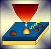
The structure and morphology of the dielectric films is typically determined by means of scanning tunneling microscopy and electron diffraction, while X-ray photoelectron spectroscopy and STM conductance spectroscopy is used to clarify composition and electronic properties. The optical response is measured via confocal laser microscopy and STM-based luminescence spectroscopy at the micro- and nanometer scale, respectively. Functionalization of the dielectric films is achieved by depositing organic molecules onto their surface, for example chromophores with potential applications in photovoltaics.
By combining various high-resolution structural and spectroscopic methods, we aim at establishing a direct, ideally atomic-scale relationship between morphology and functionality of surfaces, putting special emphasis on the role of defects and impurities. The long-term goal is hereby the clarification of elementary processes in photovoltaic, photochemical and catalytic processes, e.g. charge transfer, carrier transport and light-matter interactions.

